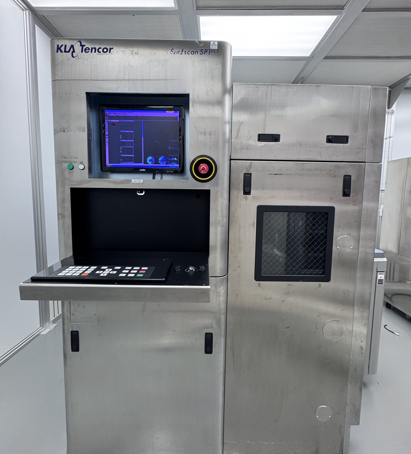
Supporting the world's installed base of legacy KLA inspection and metrology systems — from evaluation through long-term lifecycle support.
Why Legacy KLA Matters
The installed base of legacy KLA systems remains critical to mature-node semiconductor manufacturing worldwide.
As platforms age and transition beyond original support horizons, lifecycle support is increasingly important. Managing these assets requires specialized knowledge, dedicated infrastructure, and structured engineering methodologies.
Bridge Tronic Global is making disciplined investments in this technical practice to ensure these critical platforms can be supported, validated, and maintained long-term.
Platform Expertise
Dedicated technical knowledge across multiple legacy KLA product families.
Lifecycle Engineering
Engineering support from evaluation through long-term lifecycle planning.
Structured Methodology
Documented, repeatable engineering frameworks — not reactive repairs.
Factory Refurbishment
Legacy KLA Factory Refurbishment
BTG supports factory-refurbishment programs for supported legacy KLA inspection and metrology systems. Refurbishment scope is developed around the system model, configuration, condition, intended application, and customer requirements.
Supported Wafer Sizes
100 mm150 mm200 mm300 mm
Supported Technology Nodes
65 nm to 1 µm and beyond
Primary Service Regions
North AmericaEurope
BTG continues making disciplined investments in engineering talent, facility infrastructure, technical documentation, specialized tooling, and strategic technical partnerships to expand the technologies, platforms, and solutions we provide.
Supported Platforms
BTG Engineering supports multiple legacy KLA product families through dedicated platform knowledge, engineering expertise, lifecycle support, and continuous technical development.
KLA Surfscan platforms for bare-wafer and unpatterned-wafer particle, defect and haze inspection — from early cassette-to-cassette systems through the SP-generation UV platforms.
12 models
4000-5000
Surfscan 4500
Legacy cassette-to-cassette surface inspection system for 50–150 mm wafers with 200 nm PSL-equivalent sensitivity and haze measurement capability.
Wafer Size
50–150 mm (2–6 in)
Wafer Handling
Cassette-to-cassette
Illumination
HeNe laser — 633 nm
View Specifications
4000-5000
Surfscan 5000
Legacy 50–200 mm particle and haze inspection system using 633 nm HeNe illumination with 200 nm particle sensitivity.
Wafer Size
50–200 mm (2–8 in)
Wafer Handling
Cassette-based
Illumination
HeNe laser — 633 nm
View Specifications
4000-5000
Surfscan 5500
Legacy 50–200 mm Surfscan platform for particle and haze monitoring with 200 nm particle sensitivity on bare silicon and unpatterned film surfaces.
Wafer Size
50–200 mm (2–8 in)
Wafer Handling
Cassette-based
Illumination
HeNe laser — 633 nm
View Specifications
6000
Surfscan 6100
Single-puck 6000-series system covering 50–200 mm wafers with 157 nm PSL-equivalent sensitivity at 95% capture and haze measurement.
Versatile 100–200 mm inspection system rated to 150 nm at 95% capture on polished silicon, with darkfield capability across polished and high-scattering surfaces.
Wafer Size
100 / 125 / 150 / 200 mm (4 / 5 / 6 / 8 in)
Wafer Handling
Single-puck from cassette or platform
Illumination
Argon-ion laser — 488 nm
View Specifications
6000
Surfscan 6420
Refurbishable 50–200 mm platform conservatively rated to 120 nm at 95% capture and 0.02 ppm haze using low-angle darkfield illumination.
Original SP1-generation platform, commonly called SP1 Classic, with 80 nm sensitivity on polished silicon and darkfield haze capability for 150–300 mm wafers.
UV 200 / 300 mm surface inspection platform conservatively rated to the 37 nm class using 355 nm solid-state illumination and multi-mode surface quality analysis.
Wafer Size
200 / 300 mm (8 / 12 in)
Wafer Handling
Vacuum-puck; dual FIMS / FOUP on documented 300 mm configurations
Illumination
UV solid-state laser — 355 nm
View Specifications
KLA UV and ASET thin-film measurement platforms for film thickness, refractive index and reflectivity — from the UV-1XY0 series through the ASET-F5x with optional spectroscopic ellipsometry.
6 models
UV-1XY0
KLA UV-1050
Automated legacy UV thin-film metrology for 100–200 mm wafers.
Wafer Size
100, 125, 150 and 200 mm (4, 5, 6 and 8 in), configuration dependent
Wafer Handling
H2 shuttle-arm / Z-theta handler with two H-bar cassettes
Measurement Technology
Dual-beam spectrophotometry (DBS) with VTF capability
View Specifications
UV-1XY0
KLA UV-1080
Automated DBS / VTF thin-film measurement with dual-finger wafer handling.
Wafer Size
100–200 mm (4, 5, 6 and 8 in adapters), configuration dependent
Wafer Handling
Dual-finger robot with non-contact pre-aligner
Measurement Technology
Dual-beam spectrophotometry (DBS) with VTF capability
View Specifications
UV-12X0SE
KLA UV-1250SE
First-generation production UV spectroscopic ellipsometry platform.
Wafer Size
150 and 200 mm service context documented; exact supported range requires system confirmation
Wafer Handling
Automated handling; exact architecture is serial / configuration dependent
Measurement Technology
Spectroscopic ellipsometry (SE) plus DBS-family optical measurement
View Specifications
UV-12X0SE
KLA UV-1280SE
Automated UV thin-film metrology combining DBS and small-spot spectroscopic ellipsometry.
Wafer Size
100–200 mm (4, 5, 6 and 8 in adapters), configuration dependent
Wafer Handling
Dual-finger robot with non-contact pre-aligner
Measurement Technology
Dual-beam spectrophotometry (DBS) plus spectroscopic ellipsometry (SE)
View Specifications
ASET
KLA-Tencor ASET-F5
Third-generation ASET platform combining spectroscopic ellipsometry and dual-beam spectrophotometry for advanced film stacks.
Wafer Size
Up to 300 mm configurations reported; exact platen range requires confirmation
Wafer Handling
Automated open-cassette and other handler configurations; system dependent
Measurement Technology
Spectroscopic ellipsometry (SE) plus dual-beam spectrophotometry (DBS)
View Specifications
ASET
KLA-Tencor ASET-F5x
Enhanced 100–300 mm ASET platform with DBS, spectroscopic ellipsometry and optional SWE for complex film-stack characterization.
Wafer Size
100–300 mm through either 100 / 150 / 200 mm or 150 / 200 / 300 mm platen configuration
Wafer Handling
Open cassette, single / dual SMIF or single / dual FIMS; non-contact pre-alignment
Measurement Technology
DBS + SE; optional SWE, PDBS and SEEC
View Specifications
KLA OmniMap RS-Series four-point-probe sheet-resistance mapping systems for implant, diffusion, epitaxy, metals, polysilicon and bulk-substrate characterization — from manual RS-35C through automated 300 mm RS-100.
10 models
RS-35
KLA OmniMap RS-35C
Manual / tabletop configuration for semiconductor sheet-resistance mapping.
Wafer Handling
Manual tabletop loading
Temperature Compensation
No / not standard
Wafer Size
50–200 mm (2–8 in), installed chuck dependent
View Specifications
RS-55
KLA OmniMap RS-55
Manual, non-TC configuration for semiconductor sheet-resistance mapping.
Wafer Handling
Manual tabletop loading
Temperature Compensation
No
Wafer Size
Commonly up to 200 mm (8 in); installed chuck and recipes must be confirmed
View Specifications
RS-55
KLA OmniMap RS-55TC
Manual with temperature compensation configuration for semiconductor sheet-resistance mapping.
Wafer Handling
Manual tabletop loading
Temperature Compensation
Yes
Wafer Size
Commonly up to 200 mm (8 in); installed chuck and recipes must be confirmed
View Specifications
RS-55
KLA OmniMap RS-55A
Automated, non-TC configuration for semiconductor sheet-resistance mapping.
Wafer Handling
Automatic wafer loader / cassette handling
Temperature Compensation
No
Wafer Size
Up to 200 mm class; 150 and 200 mm configurations reported
View Specifications
RS-55
KLA OmniMap RS-55TCA
Automated with temperature compensation configuration for semiconductor sheet-resistance mapping.
Wafer Handling
Automatic wafer loader / cassette handling
Temperature Compensation
Yes
Wafer Size
150 and 200 mm configurations reported; other sizes require confirmation
View Specifications
RS-75
KLA OmniMap RS-75
Manual, non-TC configuration for semiconductor sheet-resistance mapping.
Wafer Handling
Manual wafer loading
Temperature Compensation
No
Wafer Size
200 mm platform well documented; smaller wafer support is configuration dependent
View Specifications
RS-75
KLA OmniMap RS-75TC
Manual with temperature compensation configuration for semiconductor sheet-resistance mapping.
Wafer Handling
Manual wafer loading
Temperature Compensation
Yes
Wafer Size
200 mm platform directly supported; smaller wafer support is configuration dependent
View Specifications
RS-75
KLA OmniMap RS-75A
Automated, non-TC configuration for semiconductor sheet-resistance mapping.
Wafer Handling
Automatic wafer loader / cassette handling
Temperature Compensation
No
Wafer Size
200 mm production configuration documented
View Specifications
RS-75
KLA OmniMap RS-75TCA
Automated with temperature compensation configuration for semiconductor sheet-resistance mapping.
Wafer Handling
Automatic wafer loader / cassette handling
Temperature Compensation
Yes
Wafer Size
200 mm production configuration directly documented
View Specifications
RS-100
KLA OmniMap RS-100
Automated 300 mm production platform configuration for semiconductor sheet-resistance mapping.
Wafer Handling
Automatic wafer loader — FOUP, open-cassette and SMIF configurations reported
300 mm standard platform; 200/300 mm configurations reported
View Specifications
KLA 8100-through-8250 CD-SEM platforms for wafer and reticle critical-dimension metrology — three series generations covering mid-1990s through early-2000s 0.13 µm production.
CD-SEMKLA 8100 SeriesMid-1990s wafer and reticle CD-SEM generation for sub-100 nm feature work at 150–200 mm wafer sizes.
The 8100 Series spans the initial wafer production platform (8100, 1995), its reticle-capable variant (8100-R, 1996), the enhanced 8100E, and the extended 8100XP / 8100XP-R generation for 0.18 µm production. Detailed configuration specifications are historical and secondary; BTG qualifies each specific system individually.
Era / Vintage
1995 through late 1990s
Primary Application
Wafer CD metrology (8100, 8100E, 8100XP); reticle / photomask CD metrology (8100-R, 8100XP-R)
Substrate / Size
Up to 200 mm wafers; reticle capability on 8100-R and 8100XP-R configurations
Specifications cited above are drawn from historical, secondary and field sources. Values are not serial-number-specific acceptance limits. Contact BTG Engineering for platform and configuration review.
CD-SEMKLA 8200 SeriesTransitional 200 mm CD-SEM generation bridging the 8100 and 8250 families for late-1990s wafer production.
The 8200 Series represents the transitional 200 mm generation preceding the well-documented 8250 family. Detailed serial-specific specifications for the 8200 are less complete in available documentation than either the 8100 or 8250 generations. BTG qualifies each specific system individually.
Era / Vintage
Late 1990s
Primary Application
200 mm wafer CD metrology
Substrate / Size
200 mm wafer platform
Process Target
Late-1990s production between 0.18 µm and 0.13 µm era
Key Capabilities
200 mm automated wafer CD production measurement
Specifications cited above are drawn from historical, secondary and field sources. Values are not serial-number-specific acceptance limits. Contact BTG Engineering for platform and configuration review.
CD-SEMKLA 8250 SeriesBest-documented 8XY0-generation platform for 0.13 µm, 200 mm wafer and reticle CD production, with Windows NT control and optional laser stage.
The 8250 Series (launched circa 2000) is the strongest-documented generation in the retained 8100-through-8250 scope. It includes the standard 8250 wafer platform, the 8250-R reticle-capable configuration, and field-documented variants. The 8250-R is documented at better than 2 nm repeatability. Exact contractual resolution, repeatability and throughput must come from final-test or site-acceptance records for each system.
Era / Vintage
Circa 2000 through early 2000s
Primary Application
0.13 µm 200 mm wafer CD production (8250); reticle / photomask CD metrology (8250-R)
Substrate / Size
200 mm wafers; reticle / photomask capability on 8250-R
Process Target
0.13 µm era production and advanced photomask characterization
Specifications cited above are drawn from historical, secondary and field sources. Values are not serial-number-specific acceptance limits. Contact BTG Engineering for platform and configuration review.
Selected discontinued KLA / Tencor stylus profilers — Alpha-Step IQ, P-Series and HRP-Series — for surface topography, step height, roughness, bow and stress measurement. Current-production KLA stylus profilers are not included.
18 models
alpha-step
KLA / Tencor Alpha-Step IQ
Legacy benchtop stylus profiler for step height, roughness and surface profiling.